Lab 1
Introduction
Lab 1 was focused on setting up, testing, and getting familiarized with the UPduino v3.1 FPGA and Nucleo-L432KC development boards. This lab entailed soldering all the necessary components and headers onto the provided E155 development board, programming the MCU and FPGA boards with Segger Embedded Studio and Radiant Lattice, respectively, and creating modules that can control LEDs and an external seven segment display. The functionality of the design portion was verified using both simulation and hardware.
Design and Testing Methodology
As shown in Figure 1, a 4-input switch will control both the seven segment display and 2 separate LEDs. The seven segment display consists of 7 LEDs that each correspond to a segment. Since the display is a common anode display, each segment will be activated when the GPIO pin that it is connected to is pulled to 0V, meaning that a value of 0 will indicate that a segment is ON. All the diodes’ anodes will be connected to 3.3V that comes directly from the UPduino, while the cathode will be connected to a GPIO pin and a current-limiting resistor. Combinational logic was used to drive LEDs 0 and 1, where led[0] = s[0] ^ s[1] and led[1] = s[2] & s[3], while LED 2 was set to constantly blink at a frequency of 2.4 Hz. This was done through the use of the built-in HSOSC (high speed oscillator) that was set to 48 MHz then divided to match the correct blinking frequency.
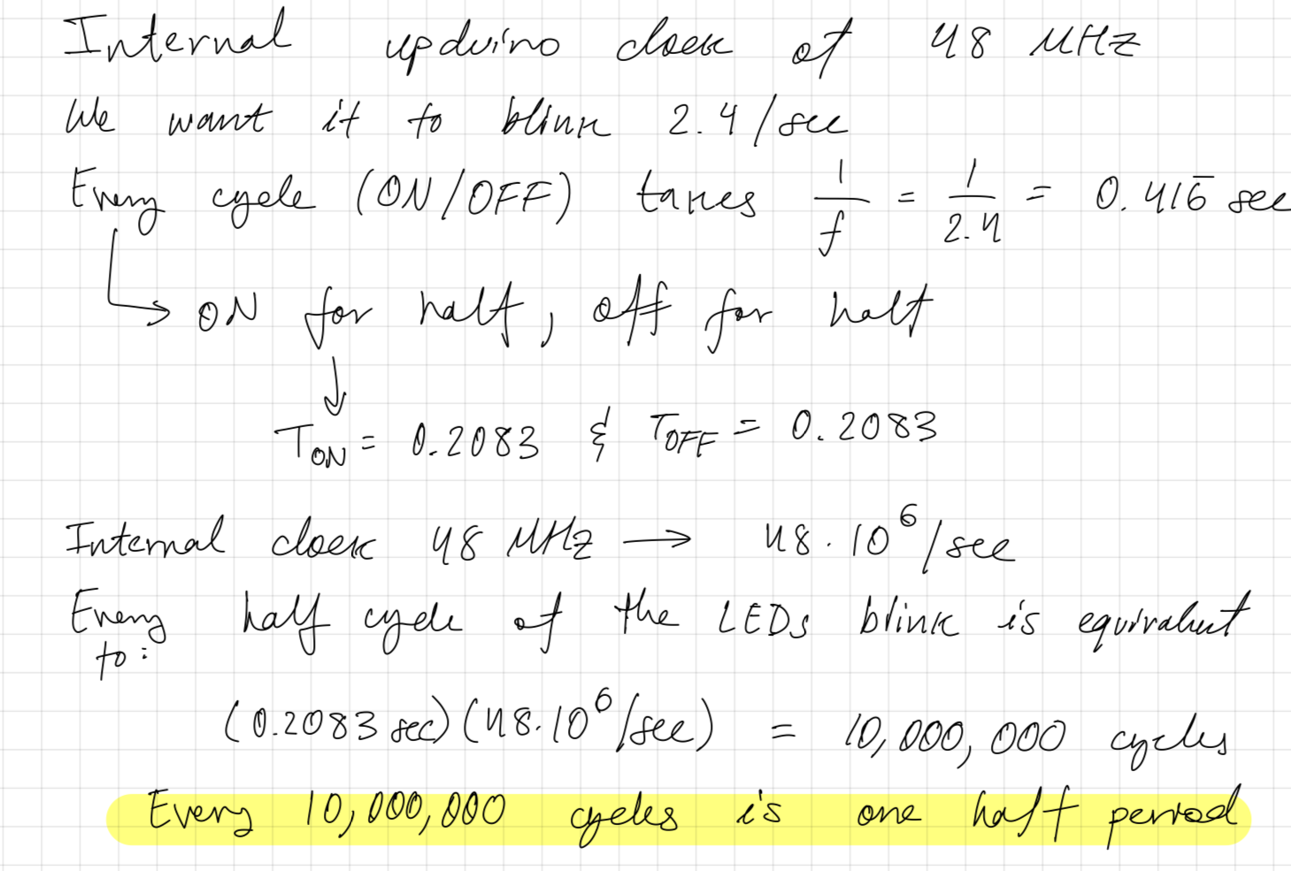
As shown in Figure 2, calculations were performed to determine how many cycles our counter would need to count to before turning off and then back on. It was determined that for 10,000,000 cycles our LED would have to be off and then on for another 10,000,000 cycles.
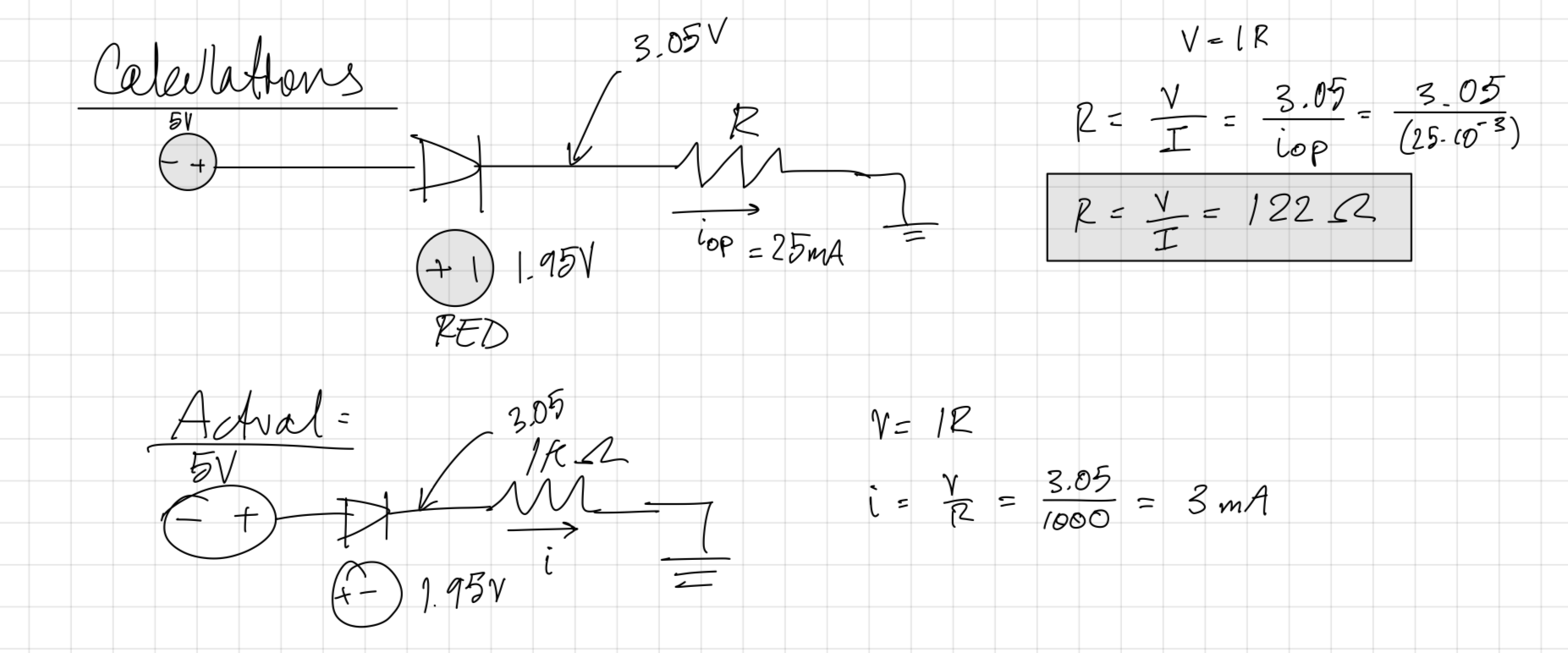
As mentioned earlier, it was important to have resistors that limit the amount of current passing through our LEDs, so the appropriate resistance was calculated using the typical operating current and forward voltage (as shown in Figure 3). It is important to note that these calculations were made using an input voltage of 5V, instead of the required 3.3V, since there were difficulties getting adequate voltage out of the UPduino’s 3.3V pin. As shown in the top half of the Figure, it is recommended to use a resistor valued at 122 ohms or greater. Given that 1000 ohm resistors were used, the actual calculations would follow the bottom half of Figure 3.
Technical Documentation:
The Git repository containing the source code of this lab can be found here: Lab 1 Repo.
Block Diagram
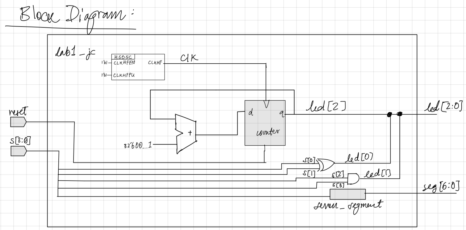
The block diagram shown in Figure 4 showcases the different modules and how they interact within the top level module. There are two inputs, s[3:0] and reset, an HSOSC module that is used to generate the clock, a counter that is used to blink LED 2, a seven_segment module containing all the combinational logic for the seven segment display, and combinational logic that is controlling LEDs 0 and 1.
Schematic
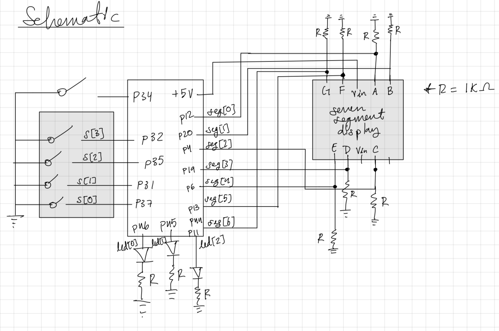
The schematic shown in Figure 5 demonstrates the hardware setup used to verify the functionality of our modules. It showcases the switches utilized to control the seven segment display and LEDs, and how it maps to the physical GPIO pins on the UPduino. The schematic illustrates the use of 1000 ohm resistors to limit the current through both the onboard LEDs and the seven segment display’s LEDs.
Results and Discussion
Testbench Simulation
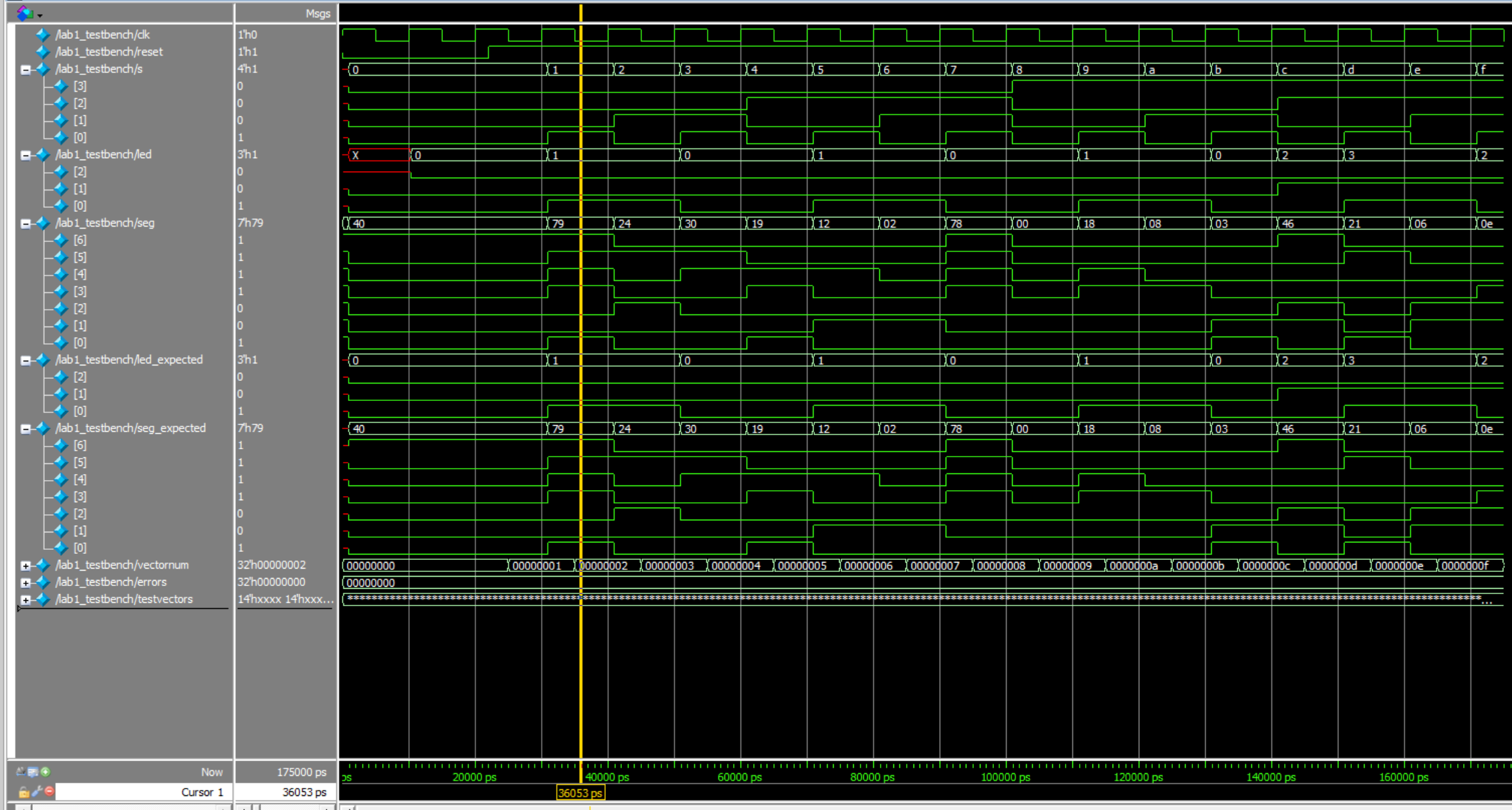
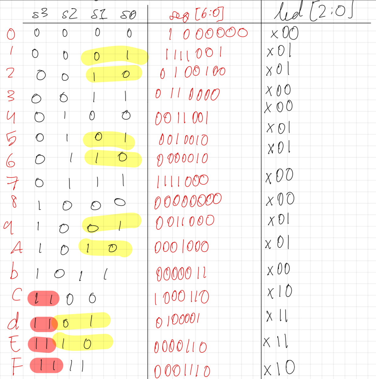
Figure 6 showcases the simulation of the lab1_jc module that is responsible for controlling both the LEDs and seven segment display. As we can see, the simulation managed to pass all 16 of the test vectors, meaning it was a successful implementation. As shown in Figure 6, the values of seg and led match their expected values, seg_expected and led_expected.
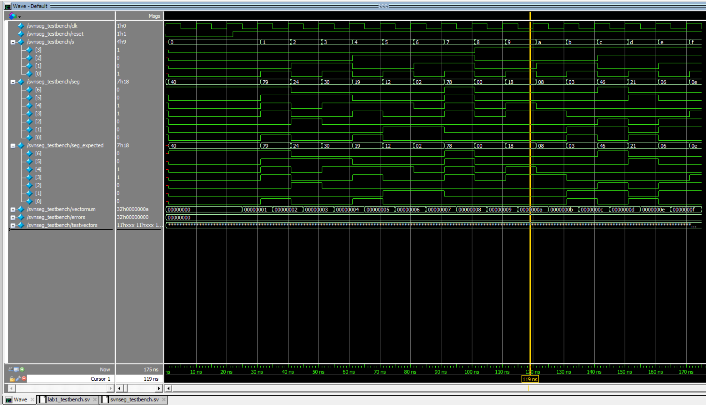
Figure 7 showcases the simulation of the seven_segment module that is responsible for controlling the seven segment display. As we can see, the simulation managed to pass all 16 of the test vectors, meaning it was a successful implementation. As shown in Figure 6, the value of seg matches the value of seg_expected.
Conclusion
The design successfully blinked led[2] using the on-board HSOSC and controlled the seven segment display, as well as led[1] and led[0] using the 4-input dip switch. Both of the testbenches that were created for their respective modules yielded great success. I spent 10+ hours working on this lab.
AI Prototype Summary

Comparing this with my own module that controls the blinking of LED 2, it is immediately clear that the syntax and structure that the LLM utilizes is not easy to read. After attempting to synthesize, the design failed immediately. The AI was unable to successfully instantiate the HSOSC module that is utilized to generate the clock. Feeding the LLM the error message, it suggested that I reorder the inputs to the HSOSC module that it attempted to instantiate. Again, this didn’t work as it should be something like: HSOSC hf_osc (.CLKHFPU(1'b1), .CLKHFEN(1'b1), .CLKHF(clk));. You would imagine that an LLM would be able to catch this simple of an issue, but it struggles. A majority of the code that the LLM produced is hard to read and/or wrong. There is also the use of language that I do not totally understand, since I am still somewhat new to Verilog. This leads me to believe there is some form of overcompensation and the LLM is making it unnecessarily complicated, since this isn’t exactly a complicated module to write. It’s shocking that the LLM is performing so terribly, but this may be due to the data that it is trained on.